|
|
Overview
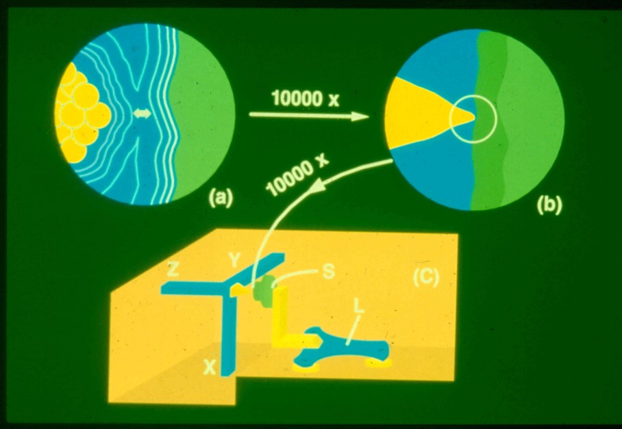
When a bias voltage is applied between a sharp tip and a sample, a quantum mechanical tunneling current can be measured if the tip is within a few atom diameters of the surface.
As a result of the quantum tunneling phenomenon, the current depends exponentially on the distance between the tip and the sample. The tip is mounted onto
three orthogonal piezoolectric elements, which allow voltages to control its position in three dimensions above the sample surface. While the tip is scanned over the
sample surface with an x-y raster, the current is amplified and measured by a feedback loop, which adjusts the z distance between the tip and sample to keep
the current constant, resulting in a constant distance between the tip and the atoms on the surface. When the scanning voltages are plotted with z as a function of
x and y, a topographic image of the surface is formed, which can be displayed as a computer image.
The STM image is always related to the electronic properties of both the tip and sample. The simple theoretical model by Tersoff and Hamann says that
the STM is sensitive to the density of states of the sample at the position of the tip. Later innovations allowed the development of scanning tunneling
spectroscopy (STS),in which the instrument is used to measure the local density of states of the sample at specific positions on the surface.
In this experiment, you will measure the atomic scale topography of graphite and gold on mica. .Measurements will probably be done at several temperatures,
such as 77K, 4.2K, and 330mK.